Single-molecule devices with low variability can be made by decoupling electronic transport and chemical attachment to the electrode.
In the past four decades, researchers have explored the use of the electronic properties of molecules to develop single-molecule devices for ultimately miniaturized electronics and extreme integration density. However, in reality, molecular electronics using single-molecule metal junctions is prone to strong variations of experimental results, requiring statistical analysis of acquired data, thus rendering practical application and industrial use almost impossible. Deviations among devices or fluctuations of the same junction originate, for example, from conformational changes of the molecules or reconfigurations of the molecule–metal contacts. These fluctuations strongly affect the electronic states of the molecular contacts and consequently the charge-carrier transport characteristics1. Though cooling of the junction reduces fluctuations, the high degree of freedom of the molecular conformation and the particular arrangement of the contacting atoms remains hard to control deterministically. Now, writing in Nature Nanotechnology, El Abbassi et al. have reported on a molecule–electrode junction where the chemical attachment of molecules to the device is decoupled from the electrical contact to the electrodes and thereby from the transport of charge carriers2.
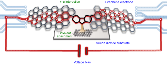
The researchers designed a molecule composed of different units with separated tasks. One unit covalently binds to the silicon dioxide substrate of the device via a silane group, providing a very stable attachment. A second aromatic unit interacts via π–π stacking with the source and drain graphene electrodes, thus controlling the charge transport (Fig. 1). These two parts of the molecule possess different chemical affinities and interact independently with different parts of the device. This configuration results in highly robust junctions with very stable current–voltage characteristics and only small current fluctuations.
Generally, the small size of molecules makes contacting them with metallic electrodes very challenging. It took almost three decades of intensive research and engineering to find ways of connecting leads to individual molecules. This first phase lasted until approximately 20103. During this period, fabrication methods for molecular contacts were established utilizing both standard lithography and bottom-up self-assembly processes. The latter is required to align molecules between the electrodes, since the molecules’ size is smaller than what top-down techniques can achieve in terms of control.
During the second phase of this evolution, researchers have engineered molecules with unique properties showing intriguing effects such as quantum interference and spin transport at the single-molecule level. Additionally, novel functions have been demonstrated such as conformational and optical switching, along with chemical sensing4,5. However, the devices typically still suffer from variations of the electrical characteristics and investigations are based on statistical analysis. One main source of the fluctuations is due to the fact that the groups ensuring the chemical connection to the device also mediate the charge transport. Vibrations alter the electronic states and can strongly affect junction characteristics.
Electrodes made out of graphene are believed to be more compatible to contact with molecules than metallic leads because they are organic and have comparable dimensions6. However, mechanical stability and electrical reproducibility are still an issue2. Therefore, the concept put forth by El Abbassi et al. to decouple binding and transport by establishing a robust covalent attachment of the molecules on the device via the silicon dioxide substrate and to realize the charge transport via π-orbital overlap of phenyl head groups is a welcome strategy to make stable single-molecule devices. As a result, they obtained highly reproducible charge transport characteristics with minimal current fluctuations of a few tenth of percent for 100 repeated current–voltage curves extending to bias voltages of up to 2V. The other important aspect is the chemical grafting of the molecule to the substrate that makes use of the chemical reactivity of the silicon dioxide substrate and fixes the position of the molecule precisely.
The assembly approach demonstrated by El Abbassi et al. has the potential to initiate a third phase in the evolution in molecular-scale electronics where junctions with negligible current fluctuations and predictable device-to-device performance are realized. If this will be the case, then practical application of molecular electronics may no longer remain elusive. The first challenge now would be the implementation of real functions, such as rectification, switching, or even recognition, in order to make use of the rich versatility of molecules and to leverage the full potential of this new assembly approach.
(원문: 여기를 클릭하세요~)
